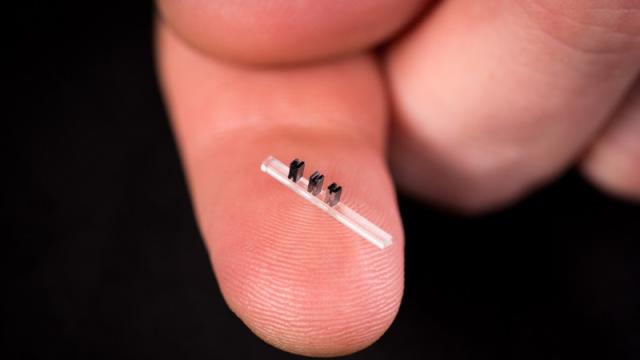
Today’s particle accelerators are massive machines, but physicists have been working on shrinking them down to tabletop scales for years. Now the Gordon and Betty Moore Foundation has awarded a $US13.5 million grant to Stanford University to develop a working “accelerator on a chip” the size of a shoebox over the next five years.
The international collaboration will build on prior experiments by physicists at SLAC/Stanford and Germany’s Friedrich-Alexander University in Erlangen-Nuremberg. If successful, the prototype could usher in a new generation of compact particle accelerators that could fit on a laboratory bench, with potential applications in medical therapies, x-ray imaging, and even security scanner technologies.
The idea is to “do for particle accelerators what the microchip industry did for computers,” SLAC National Accelerator Laboratory physicist Joel England told Gizmodo. Computers used to fill entire rooms back when they relied on bulky vacuum tube technology. The invention of the transistor and subsequent development of the microchip made it possible to shrink computers down to laptop and cell phone scales. England envisions a day when we might be able to build a handheld particle accelerator, although “there’d be radiation issues, so you probably wouldn’t want to hold one in your hand.”
There’s more than one conceptual approach to building a tabletop accelerator. The first is known as plasma wakefield acceleration, capable of accelerating electrons to very high energies over a few centimeters, compared to two miles for full-sized particle accelerators today. By firing intense, short pulses of laser light into a plasma (cloud of ionized gas), scientists can create a wave rippling through the plasma that leaves a bunch of charged particles in its wake, just like a speed boat racing across a lake churns up a wake of water in its path. Add a second laser pushing even more electrons into the plasma, and they can “surf” that wake, picking up more speed by drawing off the energy from the wakefield.
The accelerator-on-a-chip approach also employs laser, but it operates in a vacuum. While the plasma wakefield concept uses the ionized gas to provide a structure, the laser accelerator builds one out of some kind of optical material that is dielectric: something that acts as an insulator, transmitting electric force without conducting. A 2013 Nature paper described a successful prototype that used a laser to accelerate electrons through a nano structured silica glass chip smaller than a grain of rice and just 12 inches long. Those experiments successfully accelerated the electrons to near light speed, achieving rates 10 times higher than SLAC’s own linear accelerator.
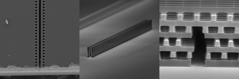
It all happens inside a tiny channel that measures less than 1/200th the thickness of a human hair. Laser light (in this case, in the infrared regime) has have electric fields that oscillate back and forth, and if the electrons are going to accelerate, they must encounter more positive electric force than retarding electric force. The physicists achieved this by etching nanoscale patterns of ridges and gaps on the channel’s walls. This increases the electric field in the ridges and reduces it in the gaps, thereby proving the electrons passing through the ridges with an energy boost. Since they only lose a bit of energy passing through the smaller gaps, they end up gaining energy.
That same year, the German physicists, led by Peter Hommelhoff, published the results of their experiments in Physical Review Letters. They achieved similar results without first boosting the electrons to near light speeds. Taken together, these two experiments demonstrated that the concept is very feasible and ripe for further development.
According to England, the idea is that everything can be made using existing micro fabrication techniques, with each individual stage of the accelerator fabricated on a single silicon wafer. Stack several of them in succession, and it will be possible to go to higher and higher energies, much like conventional accelerators use a succession of metal cavities; the more energy you want, the more such structure are required. “But our first goal is just to develop all the components and then figure out how to integrate them using a single set of fabrication steps on a single wafer,” he said.
“The chip is the most crucial ingredient, but a working accelerator is way more than just this component,” Hommelhoff (co-principal investigator of the collaboration, along with England) said in a press release. “We know what the main challenges will be and we don’t know how to solve them yet. But as scientists we thrive on this type of challenge.”
References:
Breuer, John and Hommelhoff, Peter. (2013) “Laser-based acceleration of non relativistic electrons at a dielectric structure,” Physical Review Letters 111: 134803.
Goers, A. J. et al. (2015) “Multi-MeV Electron Acceleration by Subterawatt Laser Pulses,” Physical Review Letters 115(19).
Litos, et al. (2014) “High-efficiency acceleration of an electron beam in a plasma wakefield accelerator,” Nature 515: 92-95.
Peralta, E.A. et al. (2013) “Demonstration of electron accelerationin a laser-driven dielectric microstructure,” Nature 503: 91-94.
Top image: SLAC national Accelerator Laboratory. Bottom image: Andrew Ceballos/Stanford and Chunghun Lee/SLAC.